Howdy Y'all,
I'll be driving to Philadelphia on Friday, October 24th to speak at this year's PumpCon. This lecture continues that of Black Hat USA, focusing on the exploitation--rather than the origin--of timing vulnerabilities that I've found in certain revisions of the MSP430's serial bootstrap loader.
--Travis Goodspeed
<travis at utk.edu>
Monday, September 29, 2008
Monday, September 15, 2008
Repurposing the TI EZ430U, Part 3
by Travis Goodspeed <travis at utk.edu>
of Southern Appalachia
The first installment of this series described a method of accessing the EZ430's MSP430 firmware by way of JTAG, while the second installment took a detour to discuss the TUSB3410 usb controller of the board. This third installment is concerned with the analysis of the green EZ430U firmware; that is to say, it is concerned with the firmware of the six-pin EZ430f2013 kit, which might differ from the four-pin EZ430f2013 kit and drastically differs from the red EZ430rf2500 kit.
Section 1, wherein we make general, even visual observations regarding the organization of firmware, as well as the locations of important objects.
Observe the following memory map, which was generated by the .memmap.gd.xview macro of msp430static.

In an m4s memory map, the X axis represent the less-significant byte while the Y axis represents the more significant byte. 0xFF00 would be the top left, and 0xFFFF would be the top right. As the interrupt vector table (IVT) of the MSP430f1612 ranges from 0xFFE0 to 0xFFFF, it appears as a green band in the upper right of the image. Entries within it all point to the upper red band, with addresses varying from 0xfb78 to 0xfdb0, in regular increments of 4. The only exception to this rule is the RESET vector at 0xfffe, which points to 0xfdaa.
Why such an arrangement? Each of these regularly-spaced interrupt handlers is a branch to a lower interrupt handler. The blue line that you see at the top of the black expanse is a second IVT, entries of which are called from above. 0xffe0, the DMA vector, point to a branch to &0xf7e0, which is to say that address which is contained within 0xf7e0. Similarly, 0xffe2 points to a branch to 0xf7e2. In fact, every interrupt except for RESET points to nothing but a branch to its equivalent in the table that begins 0xf7e0.
It should be clear, then, that not one but two programs reside in this image. The first-stage firmware, which rests at the top of memory, performs its own initialization when the chip is reset, but differs all interrupt handling to the lower firmware, which grows from the beginning of flash to 0xf7e0. It shouldn't be hard to instruct a compiler to build a second-stage firmware compatible with the first-stage, but it would be imprudent to spring into such a task without at least a casual analysis of the first stage.
Section 2, wherein we examine the first-stage firmware in depth.
The first-stage firmware is a bootloader which resides from 0xf800 to 0xffff in flash memory of an MSP430F1612. A quick search with MSP430static--which I'll refer to as 'm4s' for the sake of brevity--reveals that 30 functions have been found in this area. Fifteen of these, those in the range [0xfb78,0xfbb0], are merely branches to interrupt handlers in lower memory. The interrupt handler is a function which I'll call init() that resides at 0xfdaa, calling a config() function at 0xf828 to set registers to their proper values. The only call made by config() is to delay() at 0xf812 that uses nested loops to implement a timing delay.
I/O is performed by putbyte() and getbyte() functions at 0xfbc6 and 0xfbd2 respectively. These use USART0 in UART mode. This port is configured, as are many other peripherals, in the previously mentioned config() function.
As the purpose of this series of articles is to describe the process for writing a complete replacement firmware, I should mention that such information is to be found within this stage. Port 3 is especially important, as it is tied into both UARTS and I2C. As you'll recall from the early articles of this series, the TUSB3410 refuses to load with ports in the default configuration. By matching the configuration of the original firmware, we ought to be able to get something going.
To that end, Port 3 is configured as follows within the config() function.
Clocks and such must also be reconfigured, but I come bearing good news! There's an easier way, in that by relocating the IVT or reconfiguring your compiler, you can generate a custom second stage firmware without rewriting the first stage.
Section 3, wherein we examine the second-stage firmware in brief.
By comparison to the simple, neighborly firmware of the preceding section, the second stage firmware is gigantic and multi-tasking, with a rats-nest of function calls to a few key functions. Although it serves little immediate value, I'll cover second stage as an example of a few analysis techniques.
Which function calls are most popular, and what do they do? The .calls.top10 macro results in the following:
Note the sharp dropoff after the third. In a multi-tasking application, such as a TinyOS wireless sensor node, it would be logical to assume these to be mutex locks. In a JTAG adapter, however, it is much more likely that these serve an I/O purpose. Sure enough, all three are I/O related with 0x4f54 performing I/O through function calls and the other two doing it directly.
As I am not concerned with reverse-engineering the TI's proprietary debugging protocol, but rather only with making software capable of running on the EZ430 programmer, I'll delve no further into the second-stage firmware. Remember only the following: (1) That the IVT of the second-stage code resides at 0xf7e0, (2) that all else remains unchanged.
The question then becomes one of relocating the IVT, which may be accomplished either by altering linker scripts or by rewriting the firmware image before flashing it to the device. We shall begin with the prior method.
Section 4, wherein we rewrite the linker scripts of two popular compilers so as to generate our own second-stage code for this fine platform.
Moving the IVT is accomplished in GCC by forking msp430x1612.x to ez430u.x, then changing line 8 to the following:
Please note that, for no reason that I can fathom, the RESET vector of the second-stage IVT has been hard-coded to be 0x2502 in some places. You must set the .text section to begin at 0x2502, or the reset will land in the middle of a two-word instruction.
Section 5, wherein your author makes a shameless plug his upcoming appearance at the tenth annual Toorcon San Diego but provides little else of substance.
A fourth installment of this series will wrap up the replacement MSP430 code, concluding with a complete and commented `hello world' example for GCC.
of Southern Appalachia

The first installment of this series described a method of accessing the EZ430's MSP430 firmware by way of JTAG, while the second installment took a detour to discuss the TUSB3410 usb controller of the board. This third installment is concerned with the analysis of the green EZ430U firmware; that is to say, it is concerned with the firmware of the six-pin EZ430f2013 kit, which might differ from the four-pin EZ430f2013 kit and drastically differs from the red EZ430rf2500 kit.
Section 1, wherein we make general, even visual observations regarding the organization of firmware, as well as the locations of important objects.
Observe the following memory map, which was generated by the .memmap.gd.xview macro of msp430static.

In an m4s memory map, the X axis represent the less-significant byte while the Y axis represents the more significant byte. 0xFF00 would be the top left, and 0xFFFF would be the top right. As the interrupt vector table (IVT) of the MSP430f1612 ranges from 0xFFE0 to 0xFFFF, it appears as a green band in the upper right of the image. Entries within it all point to the upper red band, with addresses varying from 0xfb78 to 0xfdb0, in regular increments of 4. The only exception to this rule is the RESET vector at 0xfffe, which points to 0xfdaa.
Why such an arrangement? Each of these regularly-spaced interrupt handlers is a branch to a lower interrupt handler. The blue line that you see at the top of the black expanse is a second IVT, entries of which are called from above. 0xffe0, the DMA vector, point to a branch to &0xf7e0, which is to say that address which is contained within 0xf7e0. Similarly, 0xffe2 points to a branch to 0xf7e2. In fact, every interrupt except for RESET points to nothing but a branch to its equivalent in the table that begins 0xf7e0.
It should be clear, then, that not one but two programs reside in this image. The first-stage firmware, which rests at the top of memory, performs its own initialization when the chip is reset, but differs all interrupt handling to the lower firmware, which grows from the beginning of flash to 0xf7e0. It shouldn't be hard to instruct a compiler to build a second-stage firmware compatible with the first-stage, but it would be imprudent to spring into such a task without at least a casual analysis of the first stage.
Section 2, wherein we examine the first-stage firmware in depth.
The first-stage firmware is a bootloader which resides from 0xf800 to 0xffff in flash memory of an MSP430F1612. A quick search with MSP430static--which I'll refer to as 'm4s' for the sake of brevity--reveals that 30 functions have been found in this area. Fifteen of these, those in the range [0xfb78,0xfbb0], are merely branches to interrupt handlers in lower memory. The interrupt handler is a function which I'll call init() that resides at 0xfdaa, calling a config() function at 0xf828 to set registers to their proper values. The only call made by config() is to delay() at 0xf812 that uses nested loops to implement a timing delay.
I/O is performed by putbyte() and getbyte() functions at 0xfbc6 and 0xfbd2 respectively. These use USART0 in UART mode. This port is configured, as are many other peripherals, in the previously mentioned config() function.
As the purpose of this series of articles is to describe the process for writing a complete replacement firmware, I should mention that such information is to be found within this stage. Port 3 is especially important, as it is tied into both UARTS and I2C. As you'll recall from the early articles of this series, the TUSB3410 refuses to load with ports in the default configuration. By matching the configuration of the original firmware, we ought to be able to get something going.
To that end, Port 3 is configured as follows within the config() function.
f88e: bis.b #48, &P3SEL
f894: bis.b #16, &P3OUT
f89a: bis.b #16, &P3DIR
Clocks and such must also be reconfigured, but I come bearing good news! There's an easier way, in that by relocating the IVT or reconfiguring your compiler, you can generate a custom second stage firmware without rewriting the first stage.
Section 3, wherein we examine the second-stage firmware in brief.
By comparison to the simple, neighborly firmware of the preceding section, the second stage firmware is gigantic and multi-tasking, with a rats-nest of function calls to a few key functions. Although it serves little immediate value, I'll cover second stage as an example of a few analysis techniques.
Which function calls are most popular, and what do they do? The .calls.top10 macro results in the following:
163     4c3e    4c3e
151     4f54    4f54
142     4b6a    4b6a
29      4eca    4eca
28      6100    6100
27      2ba2    2ba2
24      8d0e    8d0e
24      a784    a784
20      5f4c    5f4c
17      756e    756e
Note the sharp dropoff after the third. In a multi-tasking application, such as a TinyOS wireless sensor node, it would be logical to assume these to be mutex locks. In a JTAG adapter, however, it is much more likely that these serve an I/O purpose. Sure enough, all three are I/O related with 0x4f54 performing I/O through function calls and the other two doing it directly.
As I am not concerned with reverse-engineering the TI's proprietary debugging protocol, but rather only with making software capable of running on the EZ430 programmer, I'll delve no further into the second-stage firmware. Remember only the following: (1) That the IVT of the second-stage code resides at 0xf7e0, (2) that all else remains unchanged.
The question then becomes one of relocating the IVT, which may be accomplished either by altering linker scripts or by rewriting the firmware image before flashing it to the device. We shall begin with the prior method.
Section 4, wherein we rewrite the linker scripts of two popular compilers so as to generate our own second-stage code for this fine platform.
Moving the IVT is accomplished in GCC by forking msp430x1612.x to ez430u.x, then changing line 8 to the following:
vectors (rw) : ORIGIN = 0xf7e0, LENGTH = 0x20Call GCC with the -T switch followed by your forked linker script, and the output will direct to the proper address. Use msp430-objdump to verify the address in your output. For further details, consult my article on Retargetting the MSPGCC Linker. In the case of the IAR compiler, the IVT range is defined near the end of lnk430F1612.xcl.
Please note that, for no reason that I can fathom, the RESET vector of the second-stage IVT has been hard-coded to be 0x2502 in some places. You must set the .text section to begin at 0x2502, or the reset will land in the middle of a two-word instruction.
Section 5, wherein your author makes a shameless plug his upcoming appearance at the tenth annual Toorcon San Diego but provides little else of substance.
A fourth installment of this series will wrap up the replacement MSP430 code, concluding with a complete and commented `hello world' example for GCC.
Monday, September 8, 2008
Errata from Black Hat USA 2008

There exist two errata, one trivial and one substantial, in my Black Hat presentation.
First, Vcc of the 2013 chip in the schematic diagram should be connected to Vcc of the JTAG/SBW connector, not Vext as is shown in the schematic. I had to score and solder those in my prototype, but I forgot to update the slides. (The new unit uses the MSP430F2274, regardless.)
Second, and much more substantially, memory is erased by default on reception of an incorrect password unless BSLKEY is set to 0x0000 on BSL version 2.0+. See page 11 of SLAA089D for details. You will find the code responsible at 0xD66 within the password comparison routine of the MSP430FG4618 Rev. G BSL, version 2.12, wherein BSLKEY is located at 0xFFBE. This makes these devices invulnerable by default, unless protection is explicitly disabled by the programmer.
The MSP430F1101A and other chips using BSL versions beneath 1.60 are vulnerable by default.
The next revision of my board will incorporate power glitching attacks, which might potentially prevent the 4618 from erasing its memory on a bad password or allow entry into a disabled BSL.
--Travis Goodspeed
Saturday, September 6, 2008
Retargetting the MSPGCC Linker
by Travis Goodspeed <travis at utk.edu>
In this article, I describe the use and modification of GCC linker scripts. In particular, I emphasize their use within MSPGCC to add support for an additional target chip, the MSP430F2274. This technique allows the generation of executables for chips which are presently unsupported by MSPGCC, as well as the creation of executables that are intended to work with a custom bootloader.
Until recently, I had been using IAR's compiler for development of the BSL Password Cracker, which was the subject of my Black Hat USA talk. IAR makes a great compiler, but the proprietary UBROF object format prevented me from exporting debugging symbols to GDB. My requests to the company for a copy of the specification have thus-far yielded nothing.
In switching to MSPGCC, I found myself unable to compile executables for the MSP430F2274 around which I had already based the second major revision of my board. In this article, I will describe a simple method for extending the MSPGCC linker to support a new chip by modifying the definition of one that's presently supported. The same technique is also handy for building an image to be compatible with a custom bootloader, as I'll describe in the next installment of my series on reprogramming the TI EZ430U with custom firmware.
Under the hood, a compiler is built of many separate applications. The first stage is a preprocessor which evaluates macros such as the #include directive. After that, the compiler stage translates preprocessed C into assembly language. A third stage, the assembler, converts assembly language into object files, which are complete except for labels that have been left empty for later insertion. A fourth stage, the linker, combines one or more object files into an executable firmware image. In the case of the MSP430, this image is a complete kernel, which does not rely upon a surrounding kernel or dynamic libraries.
As objects enter the linker, they are not quite complete machine code. This is because, prior to linking, it is impossible to know the entry address of any function. They are quite likely to be re-arranged, with unused functions stripped out entirely.
Also unknown prior to linking is the location of various system boundaries, such as the range of memory which is mapped to Flash ROM, that range which is mapped to RAM, and various ranges of lesser importance. Embedded compilers use linking scripts to specify these regions.
IAR's linker, xlink, scripts in the config/ subdirectory of each target, /opt/iar430/config on my machine but more likely C:/Program Files/IAR Systems/Embedded Workbench 5.0/430/config in Windows. Observe the code memory region of lnk430F2274.xcl as an example:
// -------------------
// Code
// -------------------
-Z(CODE)CSTART,ISR_CODE=8000-FFDD
-P(CODE)CODE=8000-FFDD
The regions themselves are helpfully described in English comments at the top of the file, giving those too lazy to read the datasheets a helping hand. It's also rather nice that these are standard command-line arguments to xlink.
GCC's linker, ld, uses a different format. Regions are described not as beginning and ending absolute addresses, but rather as an absolute beginning address and a length. The corresponding line in my 2274 script is
text (rx) : ORIGIN = 0x8000, LENGTH = 0x7fe0
The first step in retargetting the linker is to adjust the rest of the lines in the MEMORY stanza to values that work. That is nearly all the work that you must do, but converting memory regions is not quite all that you'll have to contend with. In using an MSP430F1612 script as a starting point, I initially overlooked the following line.
PROVIDE (__stack = 0x2500) ;
That line initializes the stack pointer (r1) to be 0x2500. Nothing is mapped to this address, and the entire region reads each byte as 0x5321. As GCC places globals at the bottom of memory, setting this value to the top of memory, which is to say 0x5fe, results in a functional stack.
You can find my first attempt at an MSP430F2274 linker script here. It works for me, but it comes with the usual warranty, by which I mean none. Place it in the working directory and add -T foo.x to your linking gcc line.
In the near future, I intend to add a linker-script importer for msp430static to give context to different regions of memory. Support will exist for GCC and IAR formats, and a standalone mode will allow translation between formats.
Tuesday, September 2, 2008
Speaking at Toorcon 10 in San Diego

I'll be giving a 75-minute Deep Knowledge Seminar at Toorcon X in San Diego on Friday, September 26th regarding my efforts to repurpose the TI EZ430U in-circuit debugger. This seminar will cover both of the presently published articles, as well as details on writing custom replacement firmware that will be published as a third (and perhaps fourth) installment. More generally, it will provide a thorough introduction to the reverse engineering of microcontroller-based USB peripheral boards.
Note that the seminars are not included with general conference admission. Seminar registration is $750 until September 12th, $950 at the door.
Please email me if you'd like to meet up.
--Travis Goodspeed
<travis at utk.edu>
Monday, September 1, 2008
Temporarily Paralyzing the MSP430 Memory Bus
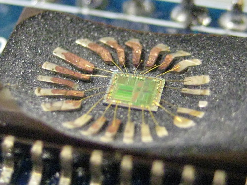
I've been playing lately with the use of light to induce temporary faults within a decapped MSP430F1101A. The chip, pictured above, was decapped by Chris of Flylogic Engineering. Lacking a convenient source of UV with which to begin erasing flash memory, I tried the flash from my digital camera. What luck!

Although it appears that flash memory has been reset, that is not in fact the case. The memory bus is paralyzed, with all reads returning 0xFFFF. This includes Flash, RAM, and ROM regions. After a while, this effect dissipates and memory returns to normal.
I'll soon begin to experiment with different wavelengths, durations, and polarizations of light. Please email me if you've any advice to offer.
Cheers,
--Travis
Subscribe to:
Comments (Atom)
